Plasma & Materials Processing
Our scientific objective is to obtain atomic-level understanding of the interaction of plasmas and reactive gases with materials in the field of atomic scale processing.

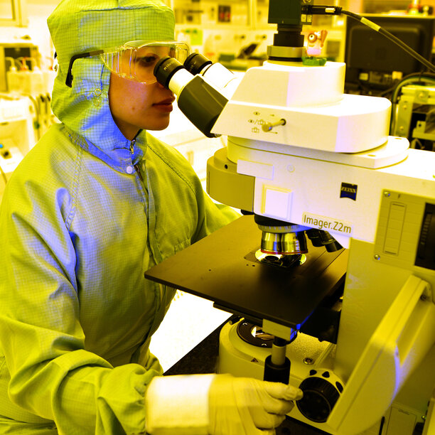
We are unique in our approach to studying plasma and surface processes in situ and in real time with a large set of current and new diagnostics
We focus on advancing the science and technology of plasma and materials processing, a multidisciplinary research area that encompasses the research fields of plasma physics, surface science and materials science. Our aim is to be an internationally leading group in the field of atomic scale processing, for present-day and future applications in energy technologies, nanoelectronics and nanotechnology.
The group studies the physics of the plasma medium, how reactive species interact with surfaces and how atomic scale processes can be used to fabricate, prepare or modify materials and their surfaces. We do so through our advanced processing facilities, our large set of plasma and surface diagnostics and state-of-the-art material analysis techniques.
News


Our PRINCIPAL INVESTIGATORS
Work with us!
Please check out the for further opportunities within our group.
Research themes

Casimir Institute
Chips and systems are the invisible infrastructure of modern life, powering AI, enabling green technologies, advancing healthcare, and driving digital transformation. The catalyzes innovation across disciplines by bringing together 700 researchers under one roof, and delivering tangible solutions for a sustainable digital information society. Located in the heart of Europe鈥檚 Brainport region, we are establishing the Chips and Systems University of Europe. Our mission is to secure Europe鈥檚 technological sovereignty by accelerating innovation in chip technologies and high-tech systems, aligned with the and the .
Inspired by Hendrik Casimir鈥檚 science-technology spiral, we embrace the reciprocal relationship between fundamental research and technological advancement. Our approach focused on future chips and high-tech systems, intertwines four key domains - design and integration, materials and processes, equipment and components, and foundational technologies into a seamless innovation engine. We deliver sustainable, high-impact innovations and develop the technologies and talent that shape the future of chips and high-tech systems worldwide.
Meet some of our Researchers
Facilities
The NanoLabTUe offers a unique combination of equipment for developing optical chips and other applications based on compound semiconductor technology.
With the facilities of the SolarLab, atomic layers can be applied to solar cells, in a quick, controlled manner, making solar cells even more efficient.
Recent Publications
Our most recent peer reviewed publications
Contact
-
Visiting address
FluxGroene Loper 195612 AP EindhovenNetherlands -
Postal address
FluxP.O. Box 5135600 MB EindhovenNetherlands -
Secretary
-
Teamlead

Education
Check out all our and our available
Are you a student interested in doing a BEP project or graduating in the Plasma & Materials Processing group? There are ample traineeship opportunities for students within our group.
If you are interested in a BEP or MSc graduation project in the PMP group, you can contact Adrie Mackus, Adriana Creatore or Erwin Kessels. It is also possible to have a lab tour if you want to orient yourself on the various possibilities.
In all projects you team up with one or more of our PhD students and staff members. You are a full member of such research team and will get a flavour of state-of-the-art atomic scale processing research.
PHOTONDELTA FAST CAREER TRACK PROGRAM
Integrated photonics will have major impact in areas such as communications, healthcare, agro-food, and mobility. The market is growing fast and thousands of jobs will be created. 黑料福利网 is the place to start a career in this field.
Do you want to be part of this future?
Then you should consider the new PhotonDelta Fast Career Track program. This program involves 黑料福利网 Master students in Applied Physics or Electrical Engineering in photonics research and applications, together with researchers and companies active in this field. For more information please consult:
PhotonDelta Fast Career Track Program for Applied Physics students
Interested? Send an email to photonicscareer@tue.nl