Photonics and Semiconductor Nanophysics
We explore the novel physics and applications emerging from the interaction of light with nanoscale matter.

Mastering light at the nanoscale
The emission and absorption of light is the physical basis of lasers, LEDs, solar cells and photodetectors, which have become crucial parts of our daily life. By controlling these processes at a subwavelength scale, we can significantly improve the performance of these photonic devices and develop completely new ones. The Photonics and Semiconductor Nanophysics group investigates the physics of (nano-)photonic structures and materials in five distinct but related research lines, mostly centered around semiconductors, for applications ranging from optical communications to sensing and energy conversion.
Read moreNews


PSN Colloquia
You can find the list of the coming PSN colloquia
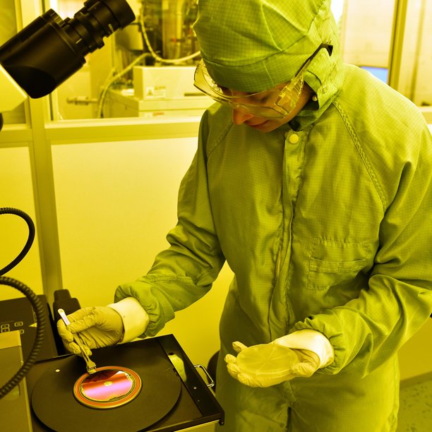
Our Labs
WORK WITH US!
Please check out the for opportunities within our group. For spontaneous applications and general inquiries, please contact prof. Jaime Gómez-Rivas.
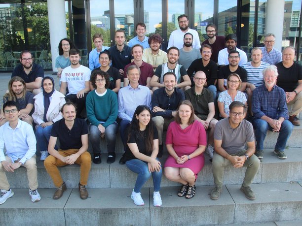
Meet some of our Researchers
Casimir Institute
Chips and systems are the invisible infrastructure of modern life, powering AI, enabling green technologies, advancing healthcare, and driving digital transformation. The catalyzes innovation across disciplines by bringing together 700 researchers under one roof, and delivering tangible solutions for a sustainable digital information society. Located in the heart of Europe’s Brainport region, we are establishing the Chips and Systems University of Europe. Our mission is to secure Europe’s technological sovereignty by accelerating innovation in chip technologies and high-tech systems, aligned with the and the .
Inspired by Hendrik Casimir’s science-technology spiral, we embrace the reciprocal relationship between fundamental research and technological advancement. Our approach focused on future chips and high-tech systems, intertwines four key domains - design and integration, materials and processes, equipment and components, and foundational technologies into a seamless innovation engine. We deliver sustainable, high-impact innovations and develop the technologies and talent that shape the future of chips and high-tech systems worldwide.

Startups
Facilities
The NanoLabTUe offers a unique combination of equipment for developing optical chips and other applications based on compound semiconductor technology.
The cleanroom at the NanoLabTUe offers a combination of equipment that is available nowhere else in the academic world. Here, optical chips based on semiconductive indium phosphide can be fabricated, from substrate right through to the end product.
The NanoLabTUe is an open-access research laboratory, in which both ���ϸ����� and other research centers and industrial parties conduct research. This approach ensures that insights and understanding acquired through fundamental research quickly find their way into industry.
Recent Publications
Our most recent peer reviewed publications
Contact
-
Visiting address
Flux, room 2.104Groene Loper 195612 AP EindhovenNetherlands -
Visiting address
Flux, room 2.104Groene Loper 195612 AP EindhovenNetherlands -
Postal address
FluxP.O. Box 5135600 MB EindhovenNetherlands -
Postal address
FluxP.O. Box 5135600 MB EindhovenNetherlands -
Secretary
Student opportunities
Check out our courses
BACHELOR AND MASTER PROJECTS
In practically all research projects there are ample opportunities for Bachelor and Master projects and internships on photonics, nanophotonics and semiconductor nanophysics. You will find all the details about the available BEP, Master and External projects of PSN in .
PHOTONDELTA FAST CAREER TRACK PROGRAM
Integrated photonics will have major impact in areas such as communications, healthcare, agro-food, and mobility. The market is growing fast and thousands of jobs will be created. ���ϸ����� is the place to start a career in this field.
Do you want to be part of this future?
Then you should consider the new PhotonDelta Fast Career Track program. This program involves ���ϸ����� Master students in Applied Physics or Electrical Engineering in photonics research and applications, together with researchers and companies active in this field. For more information please consult: PhotonDelta Fast Career Track Program for Applied Physics students
Interested? Send an email to photonicscareer@tue.nl