Advanced Nanomaterials & Devices
It is fascinating how material properties at the nanoscale can be radically changed by controlling their dimensionality, size and crystal structure. Within the AND research group, we develop novel nanomaterials and devices based on such new nanomaterials. We aim to understand the physical phenomena that take place in these materials and devices. The group is part of the Eindhoven Hendrik Casimir Institute (EHCI), which brings together the world-class photonics and quantum research at 黑料福利网 to create a unique and optimal environment to enable these fields to grow synergetically.

Fascinating nanowires and exciting research areas
We explore the unusual (quantum) properties of these new designer nanomaterials for future applications and to boost the performance of existing (opto)electronic devices. For example, topological surface states are predicted to carry dissipation-less currents and to be a precursor for new quantum states, 2D materials exhibit extraordinary ultrafast thermodynamic properties with great potential towards data communication and thermal management applications, and light-emitting SiGe will enable faster and more energy-efficient chips and connecting to distant quantum bits.
Research areas
Within our group we focus on several research areas. Areas that can be game-changers in (electronics) industry, quantum technique and quantum materials. We dive into the properties of materials, explore new methods, look into (im)possibilities of usage in applications and what value it brings. Click on the following links to learn more about each area.
Come join us on our journey!
Our work is not just about discovering new materials; it鈥檚 about redefining what鈥檚 possible.
Opportunities for Bachelor and Master Final projects
The AND group gladly welcomes motivated students intending to perform their Bachelor or Master final projects within our group. Please contact one of our PIs if you want to know more!
Come Work with us
Do you want to be part of the fundament of change and contribute to a brighter tomorrow for us all? Please check out the for further opportunities within our group.
Join us on this journey at AND, where we are shaping the technology of tomorrow.

Meet some of our Researchers
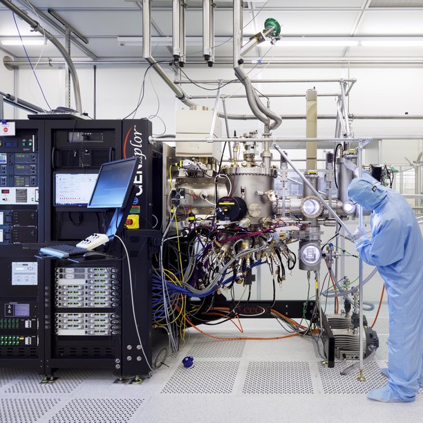
State-of-the-art Facilities
For our research we have state-of-the-art labs and equipment available:
- The NanoLab@黑料福利网 offers a unique combination of equipment for developing optical chips and other applications based on compound semiconductor technology.
- Two optics labs: one is focused on photoluminescence measurements in the visible and near-infrared range (400-1600 nm). We can do temperature dependent and time-resolved measurements. In the other lab we focus on detection of emission in the infrared range using a FTIR spectrometer.
- Thermoelectrics lab: we use two probestation set-ups in which we can measure thermal and electronic transport through individual nanowires.
- We use Metal-Organic Vapor-Phase Epitaxy (MOVPE), and Molecular Beam Epitaxy (MBE) for the growth of nanowires. We have an Aixtron Close Coupled Showerhead (CCS) for the growth of hexagonal semiconductors and an Aixtron 200/4 with 2 chambers, of which one is used for InSb and the other for InP-based semiconductors. We use a Createc MBE cluster system for the growth of III-V nanowires, II-IV-VI nanowires, and superconductors.
Recent Publications
Our most recent peer reviewed publications
News


Casimir Institute
Chips and systems are the invisible infrastructure of modern life, powering AI, enabling green technologies, advancing healthcare, and driving digital transformation. The catalyzes innovation across disciplines by bringing together 700 researchers under one roof, and delivering tangible solutions for a sustainable digital information society. Located in the heart of Europe鈥檚 Brainport region, we are establishing the Chips and Systems University of Europe. Our mission is to secure Europe鈥檚 technological sovereignty by accelerating innovation in chip technologies and high-tech systems, aligned with the and the .
Inspired by Hendrik Casimir鈥檚 science-technology spiral, we embrace the reciprocal relationship between fundamental research and technological advancement. Our approach focused on future chips and high-tech systems, intertwines four key domains - design and integration, materials and processes, equipment and components, and foundational technologies into a seamless innovation engine. We deliver sustainable, high-impact innovations and develop the technologies and talent that shape the future of chips and high-tech systems worldwide.

Education
Check out our courses
Are you a student interested in graduating or doing a project within the Advances Nanomaterials Devices group?
Join us! More information

Contact
-
Visiting address
Groene Loper 195612 AP EindhovenThe Netherlands -
Visiting address
Flux, room 2.104Groene Loper 195612 AP EindbovenNetherlands -
Postal address
Department of Applied PhysicsFluxP.O. Box 5135600 MB EindhovenNetherlands -
Secretary